
Precision Laser Processing for Semiconductor Wafers and Advanced Materials
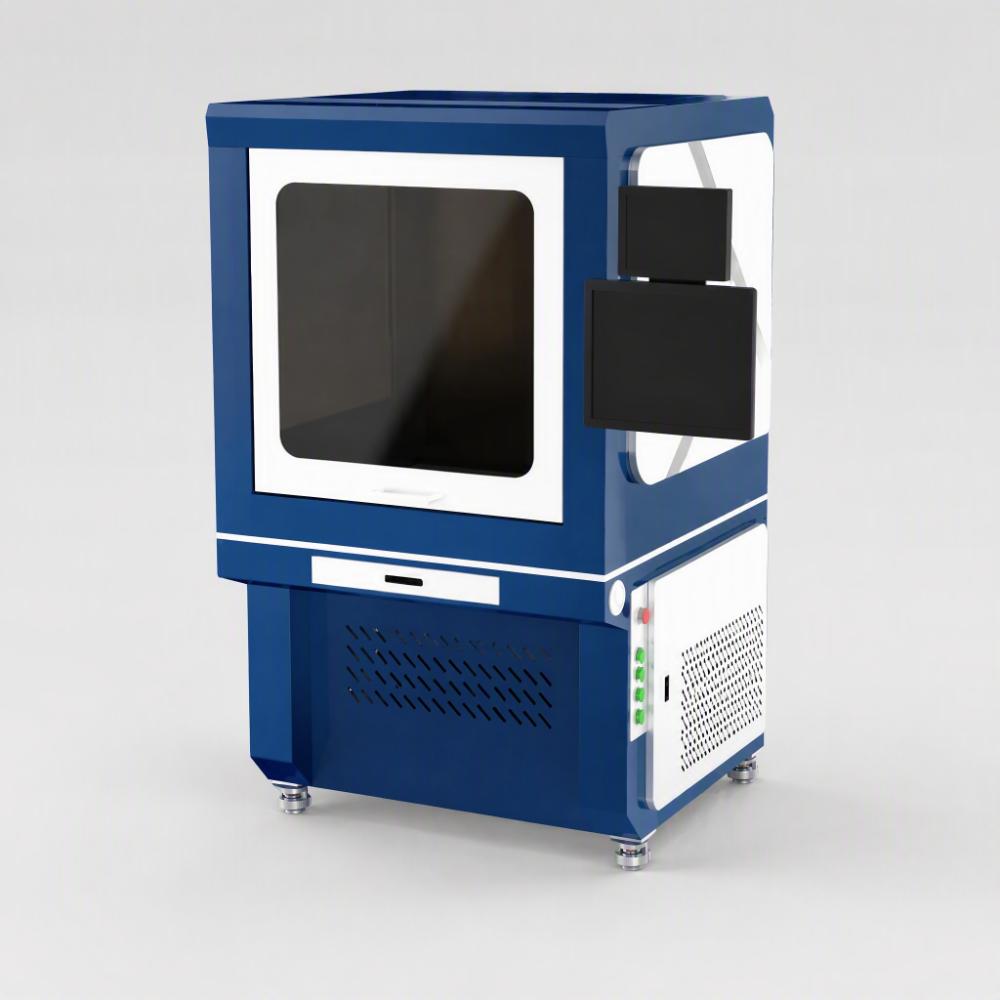
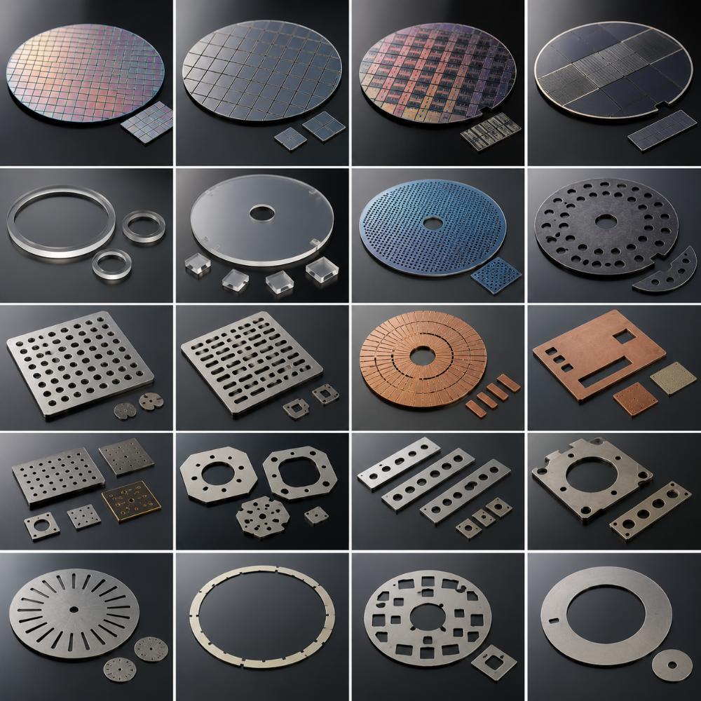
The JUYI Semiconductor & Wafer Laser Cutting Machine is a precision laser processing system designed for the cutting, scribing, separation, and micro-machining of semiconductor wafers and other advanced brittle materials.
Developed for applications that require high precision, controlled energy delivery, and repeatable processing, the system provides a flexible solution for semiconductor manufacturing, wafer processing, electronic components, optoelectronics, power electronics, and advanced material research.
Compared with conventional mechanical cutting methods, laser processing provides a non-contact machining process, reducing mechanical stress and tool wear while enabling the processing of small features, fine cutting paths, and complex wafer patterns.
The machine can be configured for different wafer materials, processing methods, laser sources, and automation requirements, making it suitable for both R&D applications and high-precision industrial production.
Key Advantages of JUYI Semiconductor & Wafer Laser Cutting Machine
1. High-Precision Wafer Laser Processing
Semiconductor wafers often require extremely controlled processing conditions because even small amounts of mechanical damage, chipping, cracking, or dimensional variation can affect downstream manufacturing processes.
The JUYI wafer laser cutting system uses a focused laser beam to process the material without direct mechanical contact.
This enables precise processing of:
- Wafer cutting lines
- Scribing lines
- Micro slots
- Small openings
- Wafer separation paths
- Customized patterns
- Precision contours
The system is designed to provide stable and repeatable processing for demanding wafer applications.
2. Non-Contact Laser Cutting Technology
Traditional mechanical cutting methods rely on physical contact between the cutting tool and wafer.
Laser cutting uses concentrated optical energy instead, creating a non-contact processing method.
Key benefits include:
- Reduced mechanical stress
- Reduced tool wear
- No physical cutting blade
- Lower risk of mechanical deformation
- Fine processing capability
- High process flexibility
- Reduced consumable tooling requirements
This makes laser processing particularly attractive for thin, brittle, fragile, or high-value semiconductor materials.
3. Suitable for Brittle and Advanced Materials
Semiconductor manufacturing increasingly involves materials with demanding mechanical and thermal characteristics.
Depending on the selected laser source and process configuration, the JUYI system can be used for processing materials such as:
- Silicon wafers
- Silicon carbide (SiC)
- Sapphire
- Gallium nitride (GaN)
- Glass
- Ceramic materials
- Compound semiconductor materials
- Other advanced semiconductor substrates
The appropriate laser wavelength and processing method should be selected according to the material’s optical absorption characteristics, thickness, crystal structure, and desired cutting quality.
4. Flexible Laser Processing Methods
Different semiconductor materials and wafer structures require different laser processing approaches.
Depending on the application, the JUYI system can be configured for processes such as:
Laser Scribing
Laser scribing creates controlled lines or weakened regions along predefined paths, allowing the wafer to be separated during subsequent processing.
Laser Ablation
High-precision laser ablation can remove localized material to create fine structures, patterns, slots, or openings.
Laser Cutting
Laser cutting can separate wafers or substrates along programmed cutting paths.
Laser Grooving
Laser grooving can create controlled grooves on semiconductor or advanced material substrates.
Precision Micro-Machining
The focused laser beam can be used for localized processing where conventional mechanical machining is difficult or impractical.
Semiconductor Wafer Applications
The JUYI Semiconductor & Wafer Laser Cutting Machine can be applied to different stages of semiconductor and advanced material processing.
Wafer Dicing
The machine can be used for laser-based wafer dicing applications where precise separation of semiconductor dies is required.
Compared with conventional blade dicing, laser processing can reduce mechanical contact and provide greater flexibility for specialized materials.
Wafer Scribing
Laser scribing is suitable for creating controlled processing lines before wafer separation.
This is particularly useful for brittle materials and applications requiring narrow processing paths.
Wafer Separation
The system can support laser-based wafer separation processes for semiconductor substrates and electronic components.
Wafer Pattern Processing
For specific applications, laser processing can be used to create localized patterns, openings, grooves, or other microstructures.
Semiconductor Substrate Processing
The machine can be configured for precision processing of semiconductor substrates used in power electronics, optoelectronics, and advanced electronic devices.
Suitable Semiconductor Materials
The actual laser configuration should be selected according to the optical and physical characteristics of the material.
Silicon (Si)
Silicon is one of the most widely used semiconductor materials for integrated circuits, sensors, power devices, and photovoltaic applications.
Laser processing can be used for wafer scribing, dicing, marking, and other precision processing applications.
Silicon Carbide (SiC)
SiC is increasingly used in high-power and high-temperature semiconductor applications.
Its high hardness and material properties can make conventional mechanical processing challenging, creating opportunities for advanced laser processing.
Typical applications include:
- Power semiconductors
- Electric vehicle electronics
- Charging systems
- Industrial power electronics
- Renewable energy systems
Sapphire
Sapphire substrates are widely used in optoelectronics, LEDs, and specialized semiconductor applications.
Laser processing provides a flexible method for precision cutting and scribing of this hard and brittle material.
Gallium Nitride (GaN)
GaN is used in high-frequency and high-power electronic devices as well as advanced optoelectronic applications.
Laser processing can be applied to selected GaN substrate and device manufacturing processes.
Glass & Ceramic Substrates
Laser technology can also be used for precision processing of selected glass and ceramic materials used in semiconductor and electronic manufacturing.
Applications in Advanced Electronics
The JUYI wafer laser cutting platform can support manufacturing applications across several advanced technology sectors.
Power Semiconductor Manufacturing
Suitable for processing semiconductor substrates and components used in:
- Power modules
- Power devices
- Inverters
- Charging systems
- Industrial power electronics
Semiconductor Packaging
Laser processing can support selected substrate, package, and component processing operations where high precision and controlled material removal are required.
MEMS Manufacturing
Microelectromechanical systems often require fine structures and precise localized material processing.
Laser micro-machining can provide a flexible solution for selected MEMS applications.
Sensor Manufacturing
Laser processing can be used for selected semiconductor and substrate processing operations involved in sensor manufacturing.
Optoelectronics
Suitable for selected wafer and substrate processing applications used in:
- LEDs
- Photodetectors
- Optical sensors
- Laser devices
- Photonic components
Photovoltaics
Laser processing technology is widely used across various stages of solar-cell and photovoltaic manufacturing.
The JUYI platform can be configured for selected wafer and substrate processing applications according to material and process requirements.
Industries Served
Semiconductor Industry
Designed for precision wafer and substrate processing in semiconductor manufacturing and research environments.
Power Electronics
Suitable for SiC, silicon, and other semiconductor materials used in high-power electronic devices.
Optoelectronics
Applicable to wafer and substrate processing for LED, photonic, optical sensor, and related applications.
Solar & Photovoltaic
Suitable for selected wafer and cell processing applications in photovoltaic manufacturing.
Advanced Materials
Can be used for research and production involving brittle and hard materials such as sapphire, ceramics, glass, and compound semiconductor substrates.
Electronics Manufacturing
Supports precision processing of semiconductor and electronic substrates used in advanced electronic products.
R&D and Universities
The flexible laser processing platform is also suitable for material research, process development, prototyping, and experimental manufacturing.
Why Choose Laser Processing for Semiconductor Wafers?
Semiconductor materials are often thin, brittle, hard, or highly sensitive to mechanical stress.
Traditional machining methods may require physical contact and specialized consumable tools.
Laser processing provides several potential advantages:
FeatureConventional Mechanical ProcessingLaser ProcessingProcessing MethodPhysical ContactNon-ContactTool WearYesNo Mechanical Cutting ToolMechanical StressRelatively HigherReducedFine Feature ProcessingLimited by Tool SizeHighly FlexibleComplex PatternsTool DependentProgram ControlledProcess FlexibilityLowerHighConsumable Cutting ToolsRequiredReducedDigital Pattern ChangeLimitedEasyAutomationAvailableHighly Suitable
Laser processing is therefore particularly valuable when manufacturers require precision, flexibility, reduced mechanical contact, and digital process control.
Flexible Automation for Wafer Processing
The JUYI Semiconductor & Wafer Laser Cutting Machine can be integrated with automated material handling and precision positioning systems according to production requirements.
Possible automation configurations include:
- Automatic wafer loading
- Precision wafer positioning
- Vision-based alignment
- Automatic laser focusing
- Programmable cutting paths
- Automatic wafer unloading
- Process monitoring
- Production data management
For high-volume manufacturing, automation can help reduce operator intervention and improve process consistency.
Vision Alignment for Precision Wafer Processing
Wafer processing often requires accurate alignment between the programmed cutting path and the wafer structure.
A vision alignment system can be integrated to identify wafer edges, alignment marks, reference points, or predefined processing locations.
This can help compensate for positioning variations and improve the accuracy of laser processing.
For applications involving complex wafer patterns or small processing features, vision-guided laser processing can provide an additional level of process control.
Typical Workflow
A typical wafer laser processing workflow can include:
Wafer Loading → Vision Alignment → Precision Positioning → Laser Processing → Inspection → Wafer Separation / Unloading
The exact workflow can be customized according to wafer material, processing method, production volume, and automation requirements.
Advantages for Semiconductor Manufacturers
The JUYI Semiconductor & Wafer Laser Cutting Machine is designed to help manufacturers address common challenges in precision wafer processing.
Reduced Mechanical Damage
Non-contact laser processing can reduce mechanical forces associated with conventional cutting tools.
High Process Flexibility
Cutting and processing patterns can be digitally programmed, allowing rapid changes between different wafer designs.
Fine Processing Capability
A focused laser beam enables localized material processing and fine cutting paths.
Reduced Tooling Requirements
Laser processing does not rely on conventional mechanical cutting blades, helping reduce mechanical tool replacement and wear-related downtime.
Suitable for Advanced Materials
The system can be configured for difficult-to-machine materials such as SiC, sapphire, ceramics, and selected compound semiconductor materials.
Automation Ready
The system can be integrated with vision positioning, automated loading/unloading, and other production automation systems.
Customized Semiconductor Laser Processing Solutions
Different wafer materials require different laser wavelengths, pulse characteristics, beam parameters, focusing methods, and processing strategies.
JUYI can develop a laser processing configuration according to the customer’s material and application requirements.
For process evaluation, customers can provide:
- Wafer material
- Wafer diameter
- Wafer thickness
- Crystal orientation
- Required cutting or scribing pattern
- Kerf width requirements
- Cutting depth
- Processing speed
- Edge quality requirements
- Production volume
- CAD drawings or sample wafers
JUYI can then recommend an appropriate semiconductor wafer laser cutting solution and processing configuration.
Technical Specifications
The exact technical configuration depends on the selected laser source, wafer material, processing method, and automation requirements.
ParameterConfigurationMachine TypeSemiconductor & Wafer Laser Cutting MachineProcessing MaterialsSilicon, SiC, Sapphire, GaN, Glass, Ceramics and other advanced substrates*Processing MethodsLaser Cutting, Scribing, Grooving, Ablation and Micro-Machining*Positioning SystemPrecision Motion Control*AlignmentOptional Vision Alignment*AutomationOptional Automatic Loading & Unloading*ApplicationWafer Cutting, Dicing, Scribing & Precision Processing
*Final specifications depend on the selected machine configuration and application requirements.
A Precision Laser Solution for Next-Generation Semiconductor Manufacturing
As semiconductor devices become smaller and advanced materials such as SiC and GaN become increasingly important, manufacturers require more precise and flexible material processing technologies.
The JUYI Semiconductor & Wafer Laser Cutting Machine provides a non-contact laser processing platform for semiconductor wafers, advanced substrates, and other precision electronic materials.
From wafer scribing and dicing to specialized micro-machining and substrate processing, JUYI can provide customized laser processing solutions based on material characteristics, production requirements, and desired processing quality.
Whether for semiconductor manufacturing, power electronics, optoelectronics, photovoltaic production, advanced materials research, or precision component manufacturing, JUYI provides flexible laser processing solutions designed for modern high-precision production.
Request a Customized Wafer Laser Cutting Solution
Looking for a semiconductor wafer laser cutting machine for your production or R&D project?
Contact JUYI with your material specifications and sample requirements. Our engineering team can evaluate the application and recommend a suitable laser source, processing method, positioning system, and automation configuration.

Reviews
There are no reviews yet.